Comparison of APS CMOS and CCD technology
As the photosensitive detector of star trackers, CCD has the characteristics of high sensitivity, wide dynamic range, uniform pixel response, etc., and has been the mainstream of star trackers for many years. The development of CMOS technology, especially APSCMOS technology and back-illuminated near-infrared CMOS technology, has made CMOS as a photosensitive detector close to the CCD level in terms of sensitivity, and some unique properties of CMOS make it more suitable for use in the aerospace field, especially star trackers. field of application.

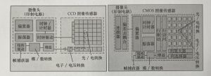
The APSCMOS photosensitive detector integrates an amplifier and readout circuit in each pixel, which is different from the charge transfer method of CCD. The charge of each pixel is read out directly through the address strobe instead of being transferred through a shift register. This characteristic makes it more resistant to radiation and has better temperature characteristics than CCD. At the same time, the processing technology is fully compatible with ordinary CMOS technology, making it easy to integrate CMOS circuits and create larger image arrays.
Star tracker rolling shutter exposure imaging method
The imaging principle of APSCMOS is very different from that of CCD. The entire frame of the CCD image is one exposure, that is, all exposure times are the same. After the exposure, each pixel is read out in sequence. In order to improve the accuracy, the photosensitive detector of the star tracker generally adopts a large area array structure, and the readout time occupies most of the image acquisition process, becoming the main limitation for improving the update rate of the star tracker. The structure of APSCMOS photosensitive detector is completely different from that of CCD. In addition to the photosensitive area, each pixel unit also has signal amplification and readout control signals. In theory, APSCMOS can directly read the response value of each pixel by accessing the memory. The readout methods of CCD and APSCMOS are as shown below.

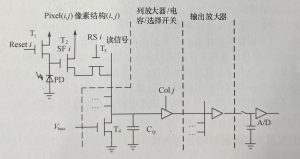
Usually the APS CMOS photosensitive unit not only contains a Photo Diode, PD but also integrates a Photo Diode Reset Transistor, Reset, Row Select Transistor, RS and a Source Follower Transistor, SF.

The image sensitive diode of APS CMOS converts the charge signal into a voltage signal. The image sensitive diode can be thought of as a capacitor. After the Reset signal is valid, the Reset power supply charges the capacitor to a level. As the light intensity and integration time increase, the voltage across the capacitor gradually decreases, forming a light sensing signal, which is amplified by SF and Isolated, and after the RS signal is valid, it is transmitted to the corresponding column amplifier for amplification and readout. Therefore, the effective integration time of the image sensitive diode is the time difference between the RS effective signal and the Reset effective signal. After RS is valid, you can reset it next time through Reset, and read it out after the next RS is valid to complete the next acquisition of light intensity. When designing the APS CMOS photosensitive detector, each row uses a Reset signal and an RS signal. That is to say, the reset time and readout time of each row are different, forming a rolling shutter imaging mode, and the exposure and readout of the sensor are performed simultaneously. When the exposure and readout time are properly designed, the frame interval time is exactly the same as the exposure time.
Send us a message,we will answer your email shortly!